We’ve covered a lot in the previous three parts of this series (see issue 67 for part one, and issue 68 for part two). If you’ve worked through them all, you should be at a point where you can create simple board designs pretty well. In the next part of this series, we are going to look at a more complex board, building a minimal RP2040 board example. The RP2040 chip itself comes in a QFN-56 package, and whilst that can be soldered at home using reflow or hotplate soldering techniques, for many, that will be a challenge too far. To avoid this, we are going to use a PCB assembly (PCBA) service.
There is a lot to look at in making an RP2040-based board, so in this article, we will prepare a simpler design for manufacture to help us learn the PCBA approach. Designing for PCBA adds complexity in that we have to create numerous files, not only defining the PCB design, but also choosing and placing known components on the board. These components have to be available to the PCB assembly house, which again adds a little complexity. It’s fair to say the first few times you do this process, it will seem like a lot of work compared to simply uploading your project file to OSH Park for it to create and send you a PCB!
So, for this exploration of PCBA services, we’ve laid out a small design in KiCad for a little H-bridge circuit prototype using four N-channel MOSFETs. We aren’t going to step through the board design, particularly as we’ve covered the approach in earlier parts of the series. You can check out the project files here.
We’re going to use the popular and reasonably affordable JLCPCB assembly service to manufacture and assemble our boards. This means that we need to consider what parts we are going to use on our board, as each part needs to be available in the JLCPCB parts library. The first thing to do is to head over to JLCPCB and register for an account. You can explore the JLCPCB parts library using the search function and filters – you will see parts’ cost and availability. In fact, you can also advance purchase components so that they are held in your own virtual warehouse ready to be used on your board designs in the future. One thing of note is that available components fall into two distinct groupings: ‘basic parts’ and ’extended parts’. Basic parts will be added to your board at the price listed. So, if you are adding five basic part resistors at 0.07 dollars each, then they will cost 0.35 per board. However, if that part was listed as an extended part, then that part will still cost the same unit price, but there will be a one-off $3 setup cost of including that part in your project, as the part will have to be manually retrieved from storage and loaded into the pick-and-place machines.

As you peruse the JLCPCB parts library, make sure that if you spot a component that you are likely to use, you make a note of the part number – these usually start with the letter ‘C’ and are listed on the main component landing page. For our small H-bridge board example, we are only interested in having JLCPCB add the SMD components, so we chose some 10 K resistors (part number C49122), and the four MOSFETs are going to be AO3400 chips (part number C20917) (Figure 2). We need to add these details to an extra field added to the Symbol Properties so that later, when we generate a bill of materials (BOM), these specific components will be identified. In order for JLCPCB to ignore the through-hole components in our design, we’ve simply not added this extra LCSC field to their schematic symbols, and therefore they won’t be included in the assembly process later on.
To add these details, in the Schematic Editor, highlight a component and press the E key to open the Symbol Properties dialog. Click the + button, which is labelled ‘Add field’ when you hover over it (Figure 3). You should see a new field line appear. In the ‘Name’ column, we need to label this field ‘LCSC’, and then in the ‘Value’ column, we need to add the CXXXXX number we researched for that component. For small projects, such as this example, you can do this manually for each schematic symbol. You need to do this for every component you expect JLCPCB to add to your board; you can’t just add this field to one 10 K resistor and expect it to work out to add the same part for the others. An alternate approach for larger projects is that you can edit the symbol at the library level, or copy the symbol to a custom library with the LCSC field and number populated at the symbol level. This means that whenever you place that custom symbol in the schematic, you have the correct LCSC part number ready for the BOM. Before creating the BOM, you still have to assign the footprints to the symbols as you would for any PCB design.

KiCad has a tool to generate a BOM – the tool icon is accessible from the Schematic Editor and shows ‘Generate a bill of materials from the current schematic’ when you hover over it. If you click this tool, it will open the Bill of Materials dialog. On the left-hand side of the dialog, you’ll see an area titled ‘BOM generator scripts’. There are some scripts already installed, but there is an excellent script written by arturo182 which specifically creates a JLCPCB-formatted BOM. To use this script, go to the GitHub repository, then in the upper right-hand corner, you will see a Download ZIP button. Click it to download, then extract the zip file (Figure 4). In the Bill of Materials dialog, click the + button and navigate into the folder you just unzipped and select the bom2grouped_csv_jlcpcb.xsl file. Clicking the OK button will add this handy script to the list.

BOM squad
Once your board is complete and you have all the LCSC numbers attached to the schematic symbols, you can reopen the BOM dialog. Select the ‘bom2grouped_csv_jlcpcb’ script, then click Generate to create a BOM that the JLCPCB service will be able to use (Figure 5).

The final piece of the PCBA puzzle is to generate a footprint position file, also referred to as a centroid file. Similar to the BOM file, this is essentially a spreadsheet which contains details of each placed component, showing both coordinates and the rotational angle of the part. To generate this, in the PCB Editor, we need to select File > Fabrication Outputs > Component Placement. Make sure that your settings match the dialog box shown in Figure 6. Note that if your project contains through-hole components that you want JLCPCB to include, you need to uncheck the ‘Include only SMD footprints’ option and include the LCSC numbers for those through-hole parts in the BOM. Note that for this component footprint POS file and the BOM file we generated earlier, we don’t want those files inside the zip file of Gerbers, as they are uploaded separately. Once you are ready, click the Generate Position File button. Notice that this will generate two POS files: one for the upper layer and one for the lower layer. As our design is single-sided, we are only interested in – and later, need to upload – the upper layer file. With the upper layer POS file generated, we need to make a few alterations to the spreadsheet column header titles for it to work properly for JLCPCB. Open the file you have generated in your spreadsheet program. We use LibreOffice Calc, but MS Excel or Google Docs should work. We need to make the following changes: the title of the first column, Ref, should be changed to Designator; PosX and PosY should be changed to Mid X and Mid Y; Rot should be changed to Rotation, and finally, Side should be changed to Layer (Figure 7). Save the POS file with these alterations – we now have everything we need to upload to the JLCPCB service.

With everything ready, we can now head to the JLCPCB website. Click on the Standard PCB/PCBA tab to upload our Gerber zip file. After a short upload, you should see a render of the upper and lower sides of your board in the preview window (Figure 8). You can make changes to the board type, material, thickness, and more on this initial page. However, apart from changing the colour of the board to yellow, we left everything at the default setting.

At the bottom of the page, you can click a button to add/expand the PCBA services. In Figure 9, you can see that we have opted to have the top side assembled only (as we only have components on this side). We’ve also ensured that the Edge Rails/Fiducials entry has the Added by JLCPCB option highlighted. This indicates that for our very small boards, JLCPCB services will create any needed panel layouts. With all that selected, click Next.


You’ll get another larger preview of the PCB layout generated from the Gerber uploads. Check it carefully and then click Next to move to the next tab. This will look like Figure 10. It’s reasonably self-explanatory. Click the Add BOM File button and upload the BOM file we created earlier, then click the Add CPL File button and upload the top layer CSV positional file we made and edited earlier. Clicking Next, these will be uploaded and processed, which may take a few minutes, and you should see a render with the board and the components placed.

Spin me round
Often, at this point, you will find that components are not rotated correctly on the footprints. There are two ways to correct this, if your components are at standard angles, you can left-click to highlight a component in the render image and, when highlighted, use the rotation tools above the PCB render in the JLCPCB web page. You can continue to do this until your design looks correct. Clicking Next will save these orientations and take you to the Add to Basket ordering page. Whilst this is a fine approach, another approach is to open the positional file we created and uploaded offline and edit the rotational value of the components that have appeared incorrectly in the render. In our experience, either way is fine, and the JLCPCB engineers will question if a component isn’t sitting on a footprint correctly.

All that’s left to do is to add the order to your shopping basket and pay! Once the order is confirmed and paid, you get regular updates on the order listing and, if it’s a complex design, it’s worth checking back into your account four to six working hours after placing the order to check the DFM analysis regarding component placing in the order history details.
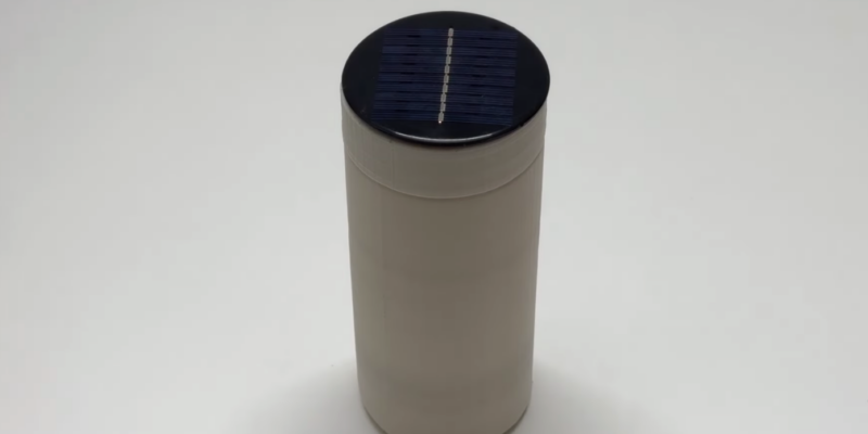
Once everything is ordered, all you have to do is wait! However, not for that long! We started this simple H-bridge motor driver design in KiCad and had the assembled PCBs (Figure 1) in our hand eight days later.